- 您现在的位置:买卖IC网 > Sheet目录492 > NTP4302G (ON Semiconductor)MOSFET N-CH 30V 74A TO220AB
�� �
�
�NTP4302,� NTB4302�
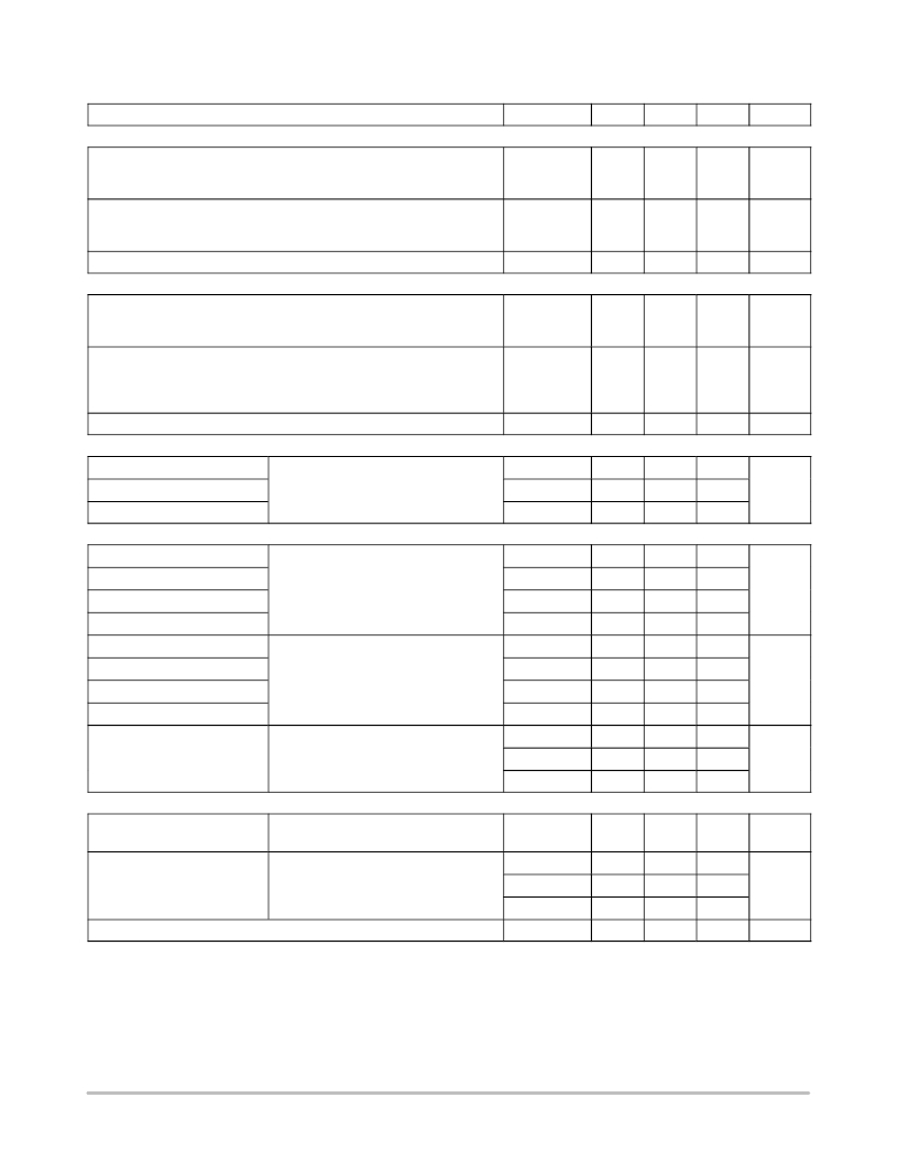
�ELECTRICAL� CHARACTERISTICS� (T� J� =� 25� °� C� unless� otherwise� noted)�
�Characteristic�
�Symbol�
�Min�
�Typ�
�Max�
�Unit�
�OFF� CHARACTERISTICS�
�Drain?to?Source� Breakdown� Voltage� (Note� 3)�
�(V� GS� =� 0� Vdc,� I� D� =� 250� m� Adc)�
�Temperature� Coefficient� (Positive)�
�V� (BR)DSS�
�30�
�?�
�?�
�25�
�?�
�?�
�Vdc�
�mV/� °� C�
�Zero� Gate� Voltage� Drain� Current�
�I� DSS�
�m� Adc�
�(V� DS� =� 30� Vdc,� V� GS� =� 0� Vdc)�
�(V� DS� =� 30� Vdc,� V� GS� =� 0� Vdc,� T� J� =� 125� °� C)�
�?�
�?�
�?�
�?�
�1.0�
�10�
�Gate?Body� Leakage� Current� (V� GS� =� ±� 20� Vdc,� V� DS� =� 0� Vdc)�
�I� GSS�
�?�
�?�
�±� 100�
�nAdc�
�ON� CHARACTERISTICS� (Note� 3)�
�Gate� Threshold� Voltage� (Note� 3)�
�(V� DS� =� V� GS� ,� I� D� =� 250� m� Adc)�
�Threshold� Temperature� Coefficient� (Negative)�
�V� GS(th)�
�1.0�
�?�
�1.9�
�?3.8�
�3.0�
�?�
�Vdc�
�mV/� °� C�
�Static� Drain?to?Source� On?Resistance� (Note� 3)�
�R� DS(on)�
�m� W�
�(V� GS� =� 10� Vdc,� I� D� =� 37� Adc)�
�(V� GS� =� 10� Vdc,� I� D� =� 20� Adc)�
�(V� GS� =� 4.5� Vdc,� I� D� =� 10� Adc)�
�?�
�6.8�
�6.8�
�9.5�
�9.3�
�9.3�
�12.5�
�Forward� Transconductance� (Note� 3)� (V� DS� =� 10� Vdc,� I� D� =� 20� Adc)�
�g� FS�
�?�
�40�
�?�
�mhos�
�DYNAMIC� CHARACTERISTICS�
�Input� Capacitance�
�C� iss�
�?�
�2050�
�2400�
�pF�
�Output� Capacitance�
�Transfer� Capacitance�
�(V� DS� =� 24� Vdc,� V� GS� =� 0� Vdc,�
�f� =� 1.0� MHz)�
�C� oss�
�C� rss�
�?�
�?�
�640�
�225�
�800�
�310�
�SWITCHING CHARACTERISTIC� S� (Note� 4)�
�Turn?On� Delay� Time�
�t� d(on)�
�?�
�10�
�18�
�ns�
�Rise� Time�
�Turn?Off� Delay� Time�
�Fall� Time�
�(V� DD� =� 24� Vdc,� I� D� =� 20� Adc,�
�V� GS� =� 10� Vdc,� R� G� =� 2.5� W� )� (Note� 3)�
�t� r�
�t� d(off)�
�t� f�
�?�
�?�
�?�
�22�
�45�
�35�
�35�
�75�
�70�
�Turn?On� Delay� Time�
�t� d(on)�
�?�
�18�
�?�
�ns�
�Rise� Time�
�Turn?Off� Delay� Time�
�Fall� Time�
�(V� DD� =� 24� Vdc,� I� D� =� 10� Adc,�
�V� GS� =� 4.5� Vdc,� R� G� =� 2.5� W� )� (Note� 3)�
�t� r�
�t� d(off)�
�t� f�
�?�
�?�
�?�
�70�
�32�
�30�
�?�
�?�
�?�
�Gate� Charge�
�(V� DS� =� 24� Vdc,� I� D� =� 37� Adc,�
�V� GS� =� 4.5� Vdc)� (Note� 3)�
�Q� T�
�Q� gs�
�Q� gd�
�?�
�?�
�?�
�28�
�7.5�
�19�
�?�
�?�
�?�
�nC�
�SOURCE?DRAIN� DIODE� CHARACTERISTICS�
�Forward� On?Voltage�
�Reverse� Recovery� Time�
�(I� S� =� 20� Adc,� V� GS� =� 0� Vdc)� (Note� 3)�
�(I� S� =� 20� Adc,� V� GS� =� 0� Vdc,� T� J� =� 125� °� C)�
�(I� S� =� 20� Adc,� V� GS� =� 0� Vdc,�
�dI� S� /dt� =� 100� A/� m� s)� (Note� 3)�
�V� SD�
�t� rr�
�t� a�
�?�
�?�
�?�
�?�
�0.90�
�0.75�
�37�
�21�
�1.3�
�?�
�?�
�?�
�Vdc�
�ns�
�t� b�
�?�
�16�
�?�
�Reverse� Recovery� Stored� Charge�
�Q� RR�
�?�
�0.035�
�?�
�m� C�
�3.� Pulse� Test:� Pulse� Width� ≤� 300� m� s,� Duty� Cycle� ≤� 2%.�
�4.� Switching� characteristics� are� independent� of� operating� junction� temperatures.�
�http://onsemi.com�
�2�
�发布紧急采购,3分钟左右您将得到回复。
相关PDF资料
NTP45N06LG
MOSFET N-CH 60V 45A TO220AB
NTP52N10G
MOSFET N-CH 100V 60A TO220AB
NTP5404NRG
MOSFET N-CH 40V 136A TO220AB
NTP5860NLG
MOSFET N-CH 60V 220A TO-220-3
NTP5863NG
MOSFET N-CH 60V 97A TO-220AB
NTP5864NG
MOSFET N-CH 60V 63A TO-220
NTP60N06LG
MOSFET N-CH 60V 60A TO220AB
NTP65N02RG
MOSFET N-CH 25V 7.6A TO220AB
相关代理商/技术参数
NTP-4401
制造商:Quest Tech. 功能描述:Connector Accessories 4 POS RJ-11 Wall Plate Ivory
NTP-4402
制造商:Quest Tech. 功能描述:Connector Accessories 4 POS RJ-11 Wall Plate White
NTP-4403
制造商:Quest Technology International Inc 功能描述:
NTP45N06
功能描述:MOSFET 60V 45A N-Channel RoHS:否 制造商:STMicroelectronics 晶体管极性:N-Channel 汲极/源极击穿电压:650 V 闸/源击穿电压:25 V 漏极连续电流:130 A 电阻汲极/源极 RDS(导通):0.014 Ohms 配置:Single 最大工作温度: 安装风格:Through Hole 封装 / 箱体:Max247 封装:Tube
NTP45N06/D
制造商:ONSEMI 制造商全称:ON Semiconductor 功能描述:Power MOSFET 45 Amps, 60 Volts
NTP45N06D
制造商:ONSEMI 制造商全称:ON Semiconductor 功能描述:Power MOSFET 45 Amps, 60 Volts
NTP45N06G
功能描述:MOSFET 60V 45A N-Channel RoHS:否 制造商:STMicroelectronics 晶体管极性:N-Channel 汲极/源极击穿电压:650 V 闸/源击穿电压:25 V 漏极连续电流:130 A 电阻汲极/源极 RDS(导通):0.014 Ohms 配置:Single 最大工作温度: 安装风格:Through Hole 封装 / 箱体:Max247 封装:Tube
NTP45N06L
功能描述:MOSFET 60V 45A N-Channel RoHS:否 制造商:STMicroelectronics 晶体管极性:N-Channel 汲极/源极击穿电压:650 V 闸/源击穿电压:25 V 漏极连续电流:130 A 电阻汲极/源极 RDS(导通):0.014 Ohms 配置:Single 最大工作温度: 安装风格:Through Hole 封装 / 箱体:Max247 封装:Tube